Oct 11, 2016
Blog Digital World New Process Uses 3-D Simulation to Create Complex Nanostructures
Designing a 3-D printed structure poses challenges, whether the product is inches or feet in size. Imagine designing one smaller than a bacterium.
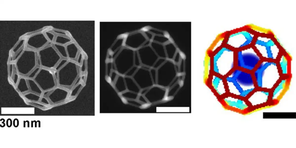
To 3-D print this impossibly small structure involves a process called focused electron beam induced deposition, or FEBID. FEBID uses an electron beam from a scanning electron microscope to condense gaseous precursor molecules into a solid deposit on a surface.
However, FEBID can be laborious, prone to errors and impractical for creating complex structures larger than a few nanometers.
But now, a powerful simulation-guided drafting process may improve FEBID while introducing new possibilities in nanomanufacturing. Developed by researchers at the Department of Energy’s Oak Ridge National Laboratory (ORNL), in collaboration with the University of Tennessee and the Graz University of Technology, the new system integrates design and construction into one streamlined process that creates complex 3-D nanostructures.
Researcher Harald Plank, who coauthored the study, says the ability to accurately design custom nanostructures “opens up a host of novel applications in 3-D plasmonics, free-standing nanosensors and nanomechanical elements on the lower nanoscale which are almost impossible to fabricate by other techniques.”
CONVERGENCE OF EXPERIMENTS AND SIMULATION
The process uses a 3-D simulation to guide the electron beam and replicate complex lattices and meshes between 10 nanometers and one micron in size. The model tracks electron scattering paths and the release of secondary electrons to predict the pattern of deposition on the surface of the material and visualize the final structure of an experiment.
According to Jason Fowlkes, a study coauthor and a researcher at ORNL’s Center for Nanophase Materials Sciences (CNMS), the innovative aspect of the work is the convergence of experiments and simulation.
The simulation guides the experimental construction, while the completed experiments, in turn, provide feedback on the accuracy and strength of the simulation. Designs are fed into the simulation and drafting program, and any inconsistencies between the two caused by secondary electron activity can be caught before the experiment.
“In its simplest form, once we know the emission profile of those secondary electrons we don’t want, we can design around them,” Fowlkes says.
Although its slower than other nanofabrication methods, only the FEBID process can produce high-fidelity 3-D nanostructures. No other methods employed by CNMS can.
Fowlkes says previous researchers who had no way to “see” the nanostructures during construction, relied on trial and error, manually adjusting the build parameters to produce the desired shapes.
He says his team now will focus on purifying the structures of carbon contamination. The purification process, called in situ purification, removes the impurities during construction. Water or oxygen and a laser are used to liberate the residual carbon from the precursor and flush it out of the structure. The simulation can even incorporate the stresses of the carbon removal process and can anticipate the transformation in the final product.
“We can design structures in a way where the actual writing pattern might look distorted, but that’s taking into account the fact that it’s going to retract and contract during purification and then it will look like the proper structure,” Fowlkes notes.
The study was published last June in ACS Nano.

From smartphones to satellites, antennas play a vital role in enabling the seaml...

Introduction Artificial Intelligence (AI) and the Internet of Things (IoT) are r...

We are your trusted research partner, providing actionable insights and custom consulting across life sciences, advanced materials, and technology. Allow BCC Research to nurture your smartest business decisions today, tomorrow, and beyond.
Contact UsBCC Research provides objective, unbiased measurement and assessment of market opportunities with detailed market research reports. Our experienced industry analysts assess growth opportunities, market sizing, technologies, applications, supply chains and companies with the singular goal of helping you make informed business decisions, free of noise and hype.