In a rapidly evolving field such as electronics, the term new is clearly relative. Most of the key materials used in today’s electronic devices have been introduced in the last few years, but new materials are being introduced continually so today’s new materials become tomorrow’s commodity materials.
For example, in chip connection technology, scientists looking to overcome its limitations have created a new light source that could enable microchips capable of handling gigabits per second data speeds. Developed by researchers at Eindhoven University of Technology, the nano-LED is 1000 times more efficient than its predecessors, they claim.
NANO-LED MAY REPRESENT NEW GENERATION OF INTERCONNECTION TECHNOLOGY
Traditional electronic materials have been pushed to their limits as advancements in technology, more sophisticated user requirements, and emerging industries have created the need for better, faster, lighter and more environmentally sustainable materials which means that entirely new material, and new device structures are required,
says BCC Research analyst Christopher Maara.
New innovations in electronic materials are supporting the need to squeeze more functionality into smaller, thinner, more flexible and aesthetically pleasing devices, with longer lasting batteries. There's also a need for these new materials to increase the density of devices as well as increase energy efficiency for computing and reliability.
The nano-LED finding may prove an answer to the bottleneck challenge posed by electronic data connections within and between microchips due to in the exponential growth of data traffic worldwide. Optical interconnects represent obvious successors, but optical data transmission like fiberglass requires an adequate nanoscale light source, which is lacking.
Not only do current on chip interconnects limit data rates, they also account for most of the energy consumed. Photonic interconnects are generally considered to be the solution, but the light source must be small enough, and with sufficient output and efficiency.
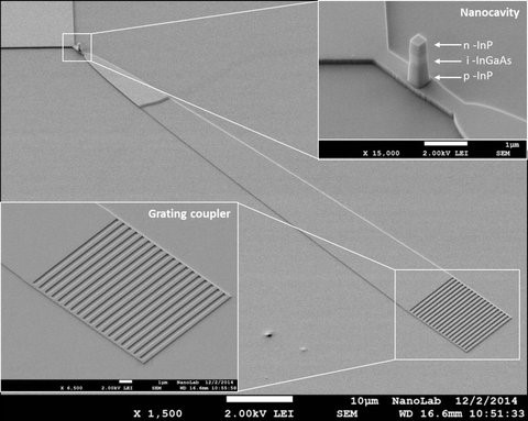
The nano-LED, which is "some hundred nanometers" with an integrated light channel to transport the light signal, consists of a metal-coated III–V semiconductor nanopillar that is said to funnel "a large fraction’ of spontaneous emission into the fundamental mode of an InP waveguide bonded to a silicon wafer."
The LED light source operates with an efficiency less than 1%, a figure the researchers claim should increase with the development of a new production method.
MEMBRANE
The nano-LED is also integrated into a silicon substrate on a membrane of indium phosphide. Silicon is the basic material for microchips, but it's not suitable for light sources unlike indium phosphide. Further tests showed that the new element converts electrical signals rapidly into optical signals and can handle data at high speeds.
A light source that converts the data into light signals which must be small enough to fit into the microscopic structures of microchips is crucial for these advancements to occur.
The researchers say that while the initial results are promising, development is not yet at the stage where it can be exploited by the industry, and the production technology has to get off the ground.


