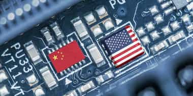
In human history many technological and scientific inventions have profoundly impacted our standard of living. In the previous century, the atom was divided into its various components and nano- and micro-technologies developed. In addition, many machines have been developed which can perform trillions of computations in a single second.
Demand for faster and smaller electronic devices remains steep. To do that, improving the integration factor per chip is the key. A critical challenge facing users of semiconductor metallization products is that mixing and matching high performance digital CMOS, analog components, MEMS and optical devices can be an expensive and risky endeavor. Users often want to create a functional prototype for testing and sampling before committing to full production tooling or custom process development.
One possible solution is mixing silicon interposers, which allows users to mix and match components in different fabrication technologies with numerous printed circuit board (PCB) implementations.
CMC Microsystems is collaborating with Innotime Technologies to develop design capability for a multi-technology interposer platform that will enable 2.5D integration of heterogeneous chip technologies in a compact physical form.
AN ECOSYSTEM FOR RAPID PROTOTYPING
Innotime's platform is designed as a simple, regular base array of through-silicon via (TSVs) with common spacing and size. The base arrays are purchased from multiple sources and are inventoried to reduce customization cycle time. Base array wafers are held in inventory prior to patterning of the top side and bottom side metallization so that prototypes can be completed rapidly in a few mask steps. This approach reduces cycle time for new designs and offers a range of wafer size and TSV performance at reasonable cost.
Innotime claims its technology platform will enable users to:
- design and manufacture a chip-scale circuit that integrates multiple chips on a single silicon substrate (bare die, bumped chips, chip-scale packages, packaged components or passives)
- customize the routing of electrical signals between them, and
- interface the assembled sub-system to the outside world using a standard ball grid array connection.
Routing between chips is managed through a circuit redistribution layer (RDL) on the interposer top surface that is user-defined using a process-specific PDK. The chips are bonded to the RDL and interposer using either wire-bonding or flip chip technology. The interposer includes TSV as a means of connecting the assembled sub-system to the package interface.
CMC will offer multi-project wafer fabrication runs for the interposer and access to flip chip assembly services that will allow users to quickly and cost-effectively develop their integrated prototypes.
The customized routing can be carried out at various laboratories and customers can choose a compatible supplier. Suppliers often have different equipment capabilities and research interests so it is up to the customer to choose a suitable supplier.
2.5 C A BOON TO TSV
2.5 IC offers a big advantage in that the die don't have to utilize the same process technology, which is a big problem with analog IP at advanced process geometries,
according to Semiconductor Engineering (SE). The site reports that "unlike full 3D-IC, which bonds wafers together, the thermal and electrical properties of 2.5D are easier to manage. Communication between chips is accomplished using interposer technology, silicon photonics, or silicon bridges."
It becomes economically harder to justify putting everything on a single system-on-chip (SoC) amid soaring design and manufacturing costs at leading-edge nodes.
“The cost of meeting Moore’s Law is increasing and the demand for performance is increasing. A portion of the roadmap now requires multi-die modules,” David McCann, vice president at California-based GlobalFoundries, the world’s second largest foundry vendor, tells Ed Sperling.
2.5D has shined best in high-end applications, according to SE. field-programmable gate arrays (FPGAs), graphics chips and networking applications have increasingly utilized the technology.
Overall, TSV or 2.5D packages should see a slight increase in usage with new products entering the graphics market, according to Ron Huemoeller, vice president of Amkor, a semiconductor product packaging and test services provider based in Pennsylvania. He
informs Mark LaPedus that "the 2.5D package space in terms of revenue will remain relatively flat in 2017 with primary usage in the high-end networking markets.”
BCC Research
expects the semiconductor metallization global market to achieve robust growth through 2021. For the inside scoop on this dynamic industry, order BCC Research's latest report
here.