Nov 1, 2015
Photonic crystal-driven sensing, which promises optical switching at speeds much higher than delivered by current technologies, is poised to realize tremendous market potential. However, for this technology to truly meet expectations, industry must forego its unwillingness and apprehension toward developing alternative fabrication methods.
The ability of photonic crystals to manipulate wavelengths based on the dielectric constant of the medium is its most potent feature. No less are its inherent properties that can be managed by altering the physical dimensions of the zones of different dielectric values.
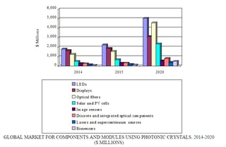
The photonic crystal component and module market comprises eight segments, including displays, optical fibers, LEDs, discrete and integrated optical components, image sensors, solar and PV cells, lasers and supercontinuum sources, and biosensors.
According to BCC Research’s Global Markets and Technologies for Photonic Crystals (PHO004B), the worldwide market for components and modules using photonic crystals is expected to reach $7.3 billion in 2015. This market is projected to grow to nearly $17.4 billion in 2020, registering a significant five-year compound annual growth rate (CAGR) of 18.9%.
The LEDs segment, the largest segment of the overall market, is expected to reach $5 billion in 2020, corresponding to a five-year CAGR of 17.6%. However, biosensors, the fastest growing segment, which should gain $426 million over the forecast period to reach $522 million in 2020, is surging at a whopping five-year CAGR of 40.3%.
But despite this growth, photonic crystals have been classic underachievers: full of promise, sound in theory, poor in implementation. They have struggled to find their place in various domains for a number of reasons, including the lack of reliable fabrication methodologies and the reluctance of industry to explore alternatives to well-oiled and well-established fabrication processes.
“The absence of a well-established roadmap for fabrication of photonic crystals remains the single, most-severe deterrent for their enhanced adoption,” says BCC research analyst Kaustubha Parkhi. “Photonic crystals are material independent. Ironically, this independence has slowed their adoption. Differences in materials lead to differences in fabrication processes. Diversity argues well for customization, but it limits short–term support, as a majority of end–use markets prefer well–proven processes to maintain operational efficiencies.”
Source: BCC Research, "Global Markets and Technologies for Photonic Crystals," September, 2015
SO WHAT’S THE PROBLEM?
The overall market CAGR of 18.9%, mentioned above, is actually a substantial downward revision from an earlier BCC forecast, which projected a CAGR of 33.1% from 2012 through 2017. While a part of this decline can be attributed to the maturing of the technology, attention should also be paid to unresolved challenges.
The major contributors for the downward revision are LEDs and solar/PV cells. These markets have undergone severe downward pricing, which has affected the overall prospects of photonic crystals as well. The challenge for solar and PV cells is compounded due to the inability of stakeholders to develop commercially sustainable deployments. Additionally, photonic crystal-enabled mobile phones are unlikely to make a major impact by 2020 due to long product development timelines and pricing factors.
These corrections notwithstanding, photonic crystals are expected to have great potential in the near future and will continue to grow in double digits.
WHY ARE PHOTONICS CRYSTALS SO PROMISING?
The ability of photonic crystals to manipulate wavelengths based on the dielectric constant of the medium is its most potent appealing feature. Photonic crystals also have properties that can be managed to a large extent by altering the physical dimensions of the zones of different dielectric values.
This attribute insulates photonic crystal fabrication from the vagaries of underlying material chemical properties to a large extent. It also provides photonic crystal device designers with the flexibility of choice in terms of material, as they need not rigidly rely on specific material.
Further, technology product designers are looking toward photonic crystals in their quest for the perfect, faster optical switch to eventually eclipse semiconductor-based technology. Indeed, optical switching is considered the proverbial Holy Grail that will influence large–scale adoption of optical circuits in domains dominated by semiconductors and electronics.
Additional benefits include the ability of photonic crystals to enhance the efficiency of existing semiconductor-based products and beyond. It is not surprising that it is the latter category that has found a more favorable reception from the industry.
Semiconductors have set a trail–blazing pace of advances over the past four decades. These advances have been instrumental in enabling these devices to conquer newer frontiers vis-à-vis operating speed, size, economy, and efficient power consumption.


We are your trusted research partner, providing actionable insights and custom consulting across life sciences, advanced materials, and technology. Allow BCC Research to nurture your smartest business decisions today, tomorrow, and beyond.
Contact Us