Whenever you use Facebook or use Google to search, the information processing happens in a large data center. The shorter the distance between optical interconnects, the better these data centers perform (think the shortest distance between two points).
To transfer information, current data systems use electrons, which can lead to bottlenecks, which can cause overheating and also wastes power.
However, using light instead of electrons to move information between computer chips and boards can improve efficiency by taking advantage of always-improving processor speeds while consuming little energy.
Researchers at the University of Washington (UW) have discovered an important first step towards building electrically pumped nanolasers (or light-based sources). These lasers are critical in the development of integrated photonic-based short-distance optical interconnects and sensors.
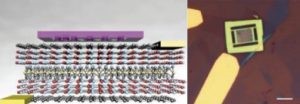
Arka Majumdar, assistant professor, and Xiaodong Xu, associate professor, both with the UW, and their team, demonstrated this first step through cavity-enhanced electroluminescence from atomically thin monolayer materials.
The material's thinness yields efficient coordination between the two key components of the laser. Both the cavity-enhanced electroluminescence and material will allow energy-efficient data centers and support high performance parallel computing.
PHOTONICS TECHNOLOGY A BOON TO OPERATIONAL EFFICIENCY
Photonics, or light-based, technology, uses light to send information, which reduces a microchip’s energy burden because light can be sent across longer distances using the same amount of power.
Light-based integrated circuits could herald huge changes in computing and network chip architecture in applications ranging from smartphones to supercomputers to large data centers.
ATOMICALLY THIN MATERIAL ENHANCES EMISSION
According to the university, recently discovered atomically thin semiconductors have drawn keen interest due to showing light emission in the 2D limit. However, because of the material's extreme thinness, its emission intensity is usually not strong enough. Thus, it's important to integrate them with photonic devices (nano-lasers, in this case) to get more light out.
Atomically thin monolayer transition metal dichalcogenides (TMDCs) are a new class of materials with strong light-matter interaction and can be easily transferred to any substrate without needing explicit lattice matching,7 emerging as a promising material system for integrated photonic applications, the researchers wrote in their report.
"Researchers have demonstrated electroluminescence in this material [atomically thin monolayer]," Majumdar explains. "Last year, we also reported the operation of an ultra-low threshold optically pumped laser, using this material integrated with nano-cavity. But for practical applications, electrically driven devices are required. Using this, one can power the devices using electrical current. For example, you power your laser pointer using an electrical battery. "
Majumdar and Xu recently reported cavity-enhanced electroluminescence in atomically thin material. A heterostructure of different monolayer materials are used to enhance the emission. Without the cavity, the emission is broadband (unidirectional) and weak. A nano-cavity enhances the emission and also enables single-mode (directed) operation. This allows direct modulation of the emission, a crucial requirement for the data-communication.
These structures are considered the new "gold rush" of condensed matter physics and materials science, according to the university. The research team's results and the previous demonstration of optically pumped lasers show the promise of electrically pumped nano-lasers, which constitutes the next milestone for this research. This next achievement will improve data center efficiency for optimal performance.
"Our team is currently exploring integration of the monolayer materials with a silicon nitride platform," Majumdar notes."Through this work, we hope to achieve the coveted CMOS [complementary metal-oxide-semiconductor] compatibility, which is the same process by which the computer processors are fabricated today."


