As the digital revolution continues to exponentially expand, it's also shrinking in some ways. How's that for irony?
Skyrocketing network demands, unyielding data accumulation, and clamoring for bigger bandwidth pipes require ever more efficient solutions with higher power densities and high-speed designs while preserving signal integrity.
More, more, more. Understandably.
The response of interconnection technology to all this furious howling?
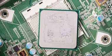
Get smaller. Miniaturize. Reduce footprint. Indeed, in the realm of PCB technology, the trend toward the miniaturization of printed circuit boards and IC substrates, in addition to the extensive integration of functions is, well, expanding.
And with it, the combination of production processes and materials for high-end printed circuit boards with processes and technologies from IC substrate production is yielding further potential for miniaturization.
Against this backdrop, an Austrian-based printed circuit board designer and manufacturer has rolled out a "
toolbox" that offers a range of high-end technologies that can be combined with each other for miniaturization on all interconnection layers.
The AT&S Toolbox uses technologies such as insulated metallic substrate (IMS), multilayer, HDI, any layer, wire-bond-board, flexible PCBs, chip embedding, IC substrates and interposers. The assembly service sector and the packaging market are particularly worth mentioning here. The additional integration of components in substrates and printed circuit boards (embedded component packaging) can significantly reduce measurements in all dimensions, the company claims.
This means for modern SIPs (system in packages) that conductor track widths/spacings of 15 µm are possible and significantly less than 10 µm for IC substrates. New high-end systems such as advanced SIPs and SiBs (system in boards) can be combined in modular form with all basic technologies. This flexibility allows customers to optimize their solutions with specific applications.
“PCBs will feature ever more advanced packaging solutions," says Andreas Gerstenmayer AT&S CEO. " With our AT&S Toolbox, we are perfectly equipped to combine the various technologies in modular and intercompatible concepts. Miniaturization trends can be implemented efficiently on all layers.”
From a small seed a mighty trunk will grow.